USB Interface & Serialiser hardware
I don't use this system at all but it documents the beginning of my DATV Experience!
Created March 2009, minor updates Jan 2010
This page explains my USB interface to the Digital ATV Transmitter, this is only one part of the system and the rest is very much the same as the original F4DAY design that is shown on the other pages. Basically it takes the USB data stream in from the PC and converts it into base band IQ signals ready for driving an IQ modulator.
The basics of the system are shown below, ideally there needs to be some filtering of harmonics etc but it works!
DATV System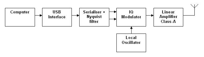
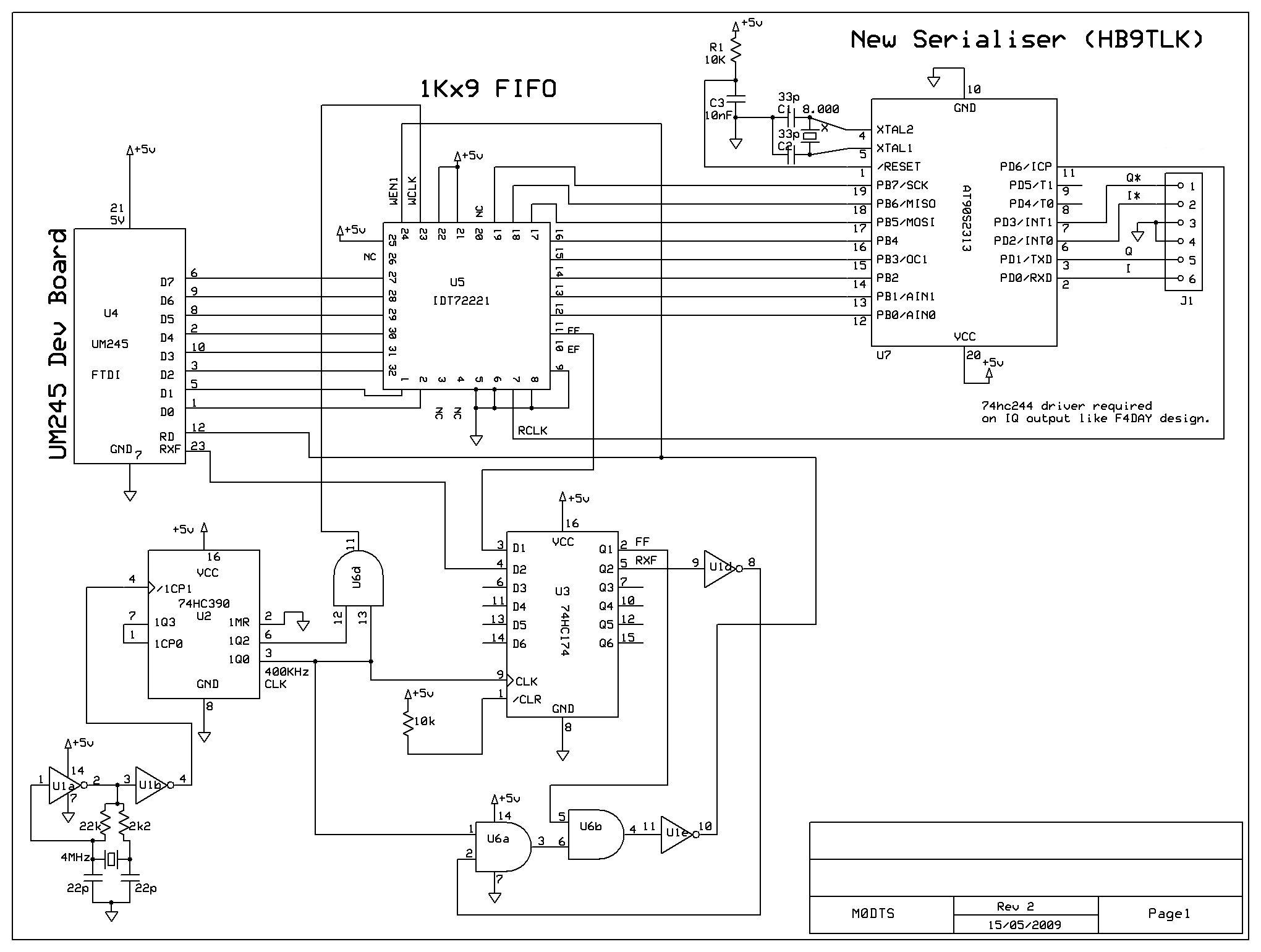
USB Interface & Serialiser
Thanks to Cesco HB9TLK for his implementation of a new serialiser chip I have now managed to send Digital ATV from pre-recorded files using the USB port of the pc rather than the parallel port in the original design, The information is below and now seems to be stable.
The new version of the serialiser incorporates part of the software process to reduce the required bandwidth to the transmitter - this is the Viterbi decoder and it reduces the data sent to the serialiser by half, so for 1024 symbol rate it only requires 1024Kb/s transfer rate from the pc rather than the 2048Kb/s with F4DAY serialiser, this makes it easier to accomplish with a USB interface. It also uses an Atmel 2313 chip which is a lot cheaper and in a more user friendly package!
The USB interface is based around the FT245 USB<>Parallel FIFO chip and provides a buffered data stream via the USB bus to the serialiser. This is far easier than the original design which used the pc parallel port and DOS to make it work correctly.
The main problem with using the USB bus is the interrupts in the data flow, these cause some bytes to be lost and corrupts the overall data output of the FT245 if it is being used at high data rates. This is just a rough guess but I think that about 64KB/s is about the limit for loss less transfer, above that I see the RXF flag start to show that the FT245 FIFO is running empty. The TX buffer on the FT245 is 128 bytes and this is obviously not enough for the high data rates that is says it can achieve on its own.
At 128KB/s I noticed *up to* 1.5mS gaps on the RXF pin at random time intervals, by calculation you can see that this is 0.0015Seconds x 128000Bytes = 192 Bytes gaps, this is more bytes lost than the FIFO buffer is capable of holding so some erroneous data was still being read if the serialiser was connected directly to the FT245 chip.
The TX FIFO buffer in the FT245 is 128Bytes so when there is an interrupt the buffer can be empty briefly and no data could be read from the device, the data that is needed for the serialiser is a continuous stream without any gaps. To fix this problem I have used another FIFO buffer in-between the FT245 and the serialiser, the buffer is 1K bytes long so in theory I should be able to transfer more than 2Mb/s?. not tested yet!
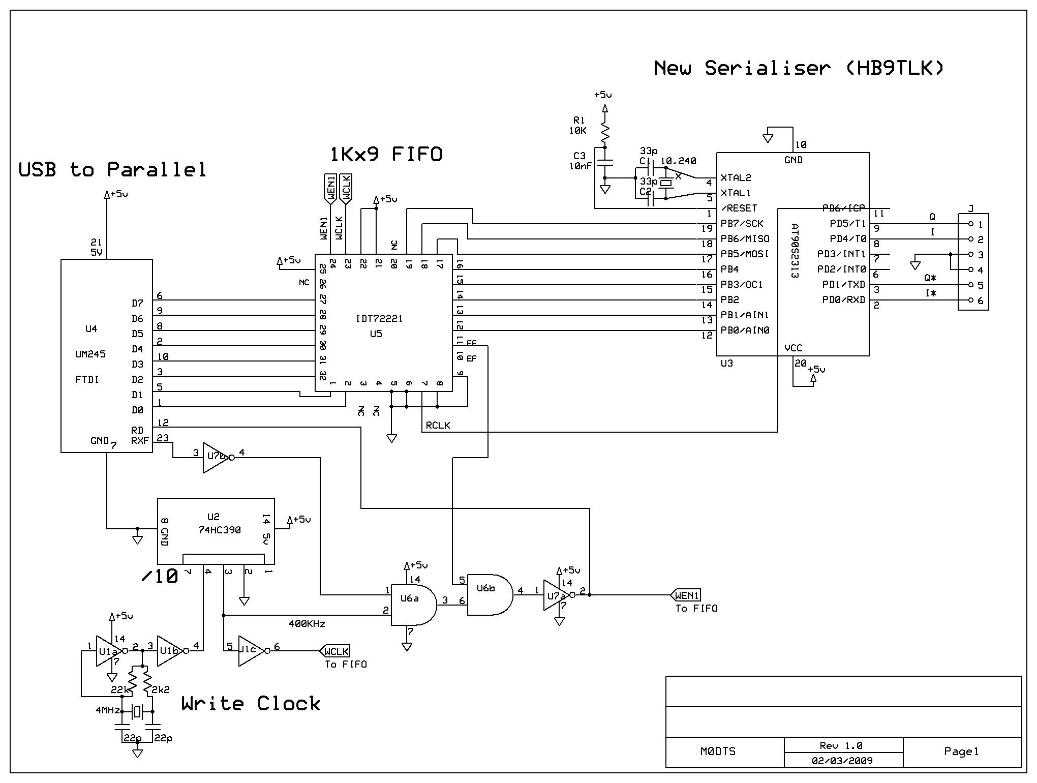
To control the clocking of each byte of data from the FT245 into the FIFO chip I had originally used a PIC16F84 but this proved to be too slow if I wanted to do higher data rates than 1024Kbit/s. I have since replaced this with some logic gates and another oscillator as seen in the schematic below
All of the parts mentioned are available from Farnell in one off pieces.
FT245:
The RD pin is pulled low to load a new byte of data on the FT245 parallel port.
The RXF pin goes high when there is no data available on the FT245
FIFO:
FF goes low when the fifo is not full.
WEN1 needs to go low before WCLK to enable a valid write to the fifo.
WEN1 is tied to RD so that a byte is presented on the FT245 parallel port before WCLK
WCLK is the main Write clock to the fifo, is triggered on falling edge also.
The above effectively only lets a byte be written to the fifo if the fifo is not full and there is a byte available on the FT245, the main write clock runs quite fast on my test circuit @400KHz to overcome the data gaps up to and probably above 2Mb/s.
I guess any FIFO chip could be used as long as it can read and write at the same time at different clock speeds.
See F1FAU design on http://www.netonoff.com for another example of a USB interface.
Data can be sent to the serialiser through a Windows program that I wrote in Visual Basic or with the Live software solution in Linux on the other page.
The Windows software can be downloaded from here soon!
Hopefully in the not too distant future I would like to make a new PCB layout to give IQ output from USB data input, I also hope to re-design the modulator board and possibly build it all onto one board so that we can have USB in and RF out!?.. We shall see if I get time to do all that!
Currently I do not have any of the displayed pcb layouts available; they are not really much use in the form they are with my old software, however I am working on some updated schematics/layouts with Eagle software but they will not be ready for some time ? Jan 2010
Updated Schematic V3 of USB Serialiser 27th Feb 2010 - Click to enlarge
Currently working well to 2Mbit
This update includes the option to generate IQ test signals to help setup the modulator and reduces the component count considerably by using another AVR chip.
Hex file for the ATtiny13 is here - Program with no clock divider and INT 9.6MHz clock
Hex file for the ATtiny2313 is here - Program with no clock divider and EXT crystal
V3 FIFO Interface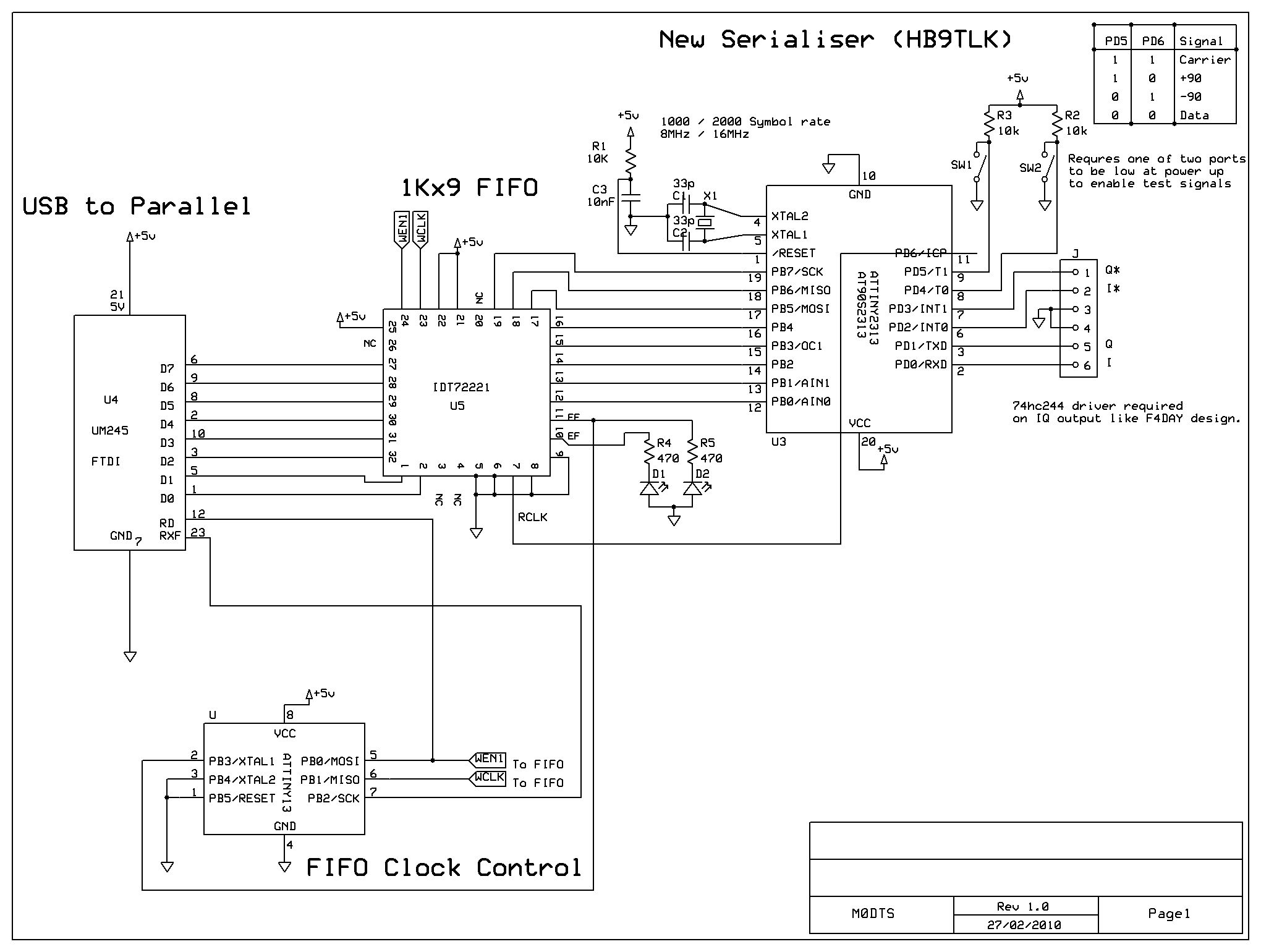
*** 7th Feb 2010 - noticed IQ outputs where wrong.. I/Q were swapped with I*/Q* V2 Schematic updated ***
*** Nov 2010 - Thanks to Alain F1CJN for reporting that i had missed two ground connections on the TINY13 (PB4+PB5) - V3 Schematic updated ***
Old Version V2
Old version V1
Here are some hints/tips for when you build the system!!
Serialiser:
* ATTiny2313 needs to be programmed with no divider setting in the fuses. With an 8MHz crystal fitted you should see 125 KHz on pin11 once programmed correctly. ( or 250KHz if you have a 16MHz crystal fitted)
* You should see a few hundred Kilohertz clock permanently on the WCLK pin of the FIFO chip or Pin 6 of the Attiny13
* The WEN1 pin of the FIFO will show as intermittent activity when sending data via USB port and not a constant rate. The FIFO only accepts new data when it?s available from the FT245. WEN1 will be held high when RXF is low on the FT245.
* The /EF and /FF flags on the FIFO give a good indication of correct operation, I used 470R from each line to an LED to ground, both LED?s will be lit continuously when data is being sent from the pc at or above the serialiser rate.
If /EF is low then the problem is related to the read clock from the Attiny2313. If /FF pin is low then it could be no data being sent to USB device or a fault with the write clock circuit (Attiny13). If the LEDs are fairly Intermittent it usually means there is not enough data being sent to the USB device from the pc, wrong symbol rate etc?
* At I/Q inputs to modulator you should see around +2.4v with a multimeter when sending data, there may be a small difference between I and Q measurements.
* Using oscilloscope with X-Y function connected to I and Q from the Nyquist filter you should see the square constellation pattern similar to the one shown below.
Modulator:
* The IQ gain/balance adjust pot?s are both roughly 1/3 turn clockwise from Left stop, this should give equal gain and good enough balance for your first tests.
* The IQ bias adjust pot?s are dependant on the operating frequency but only degrade the performance of the system by a small amount; I find they are normally no more than 1/2 turn clockwise from left stop but usually slightly different positions for best LO suppression, your settings maybe different but you should be able to notice a significant change in the level of the carrier. I can not detect the carrier while I can hear digital noise once it?s set on my system.
* The LO suppression can now be done using the new test mode switches on the serialiser. If you do not have a spectrum analyser then the best way to set the LO suppression is with another receiver on USB tuned 1 KHz low of the LO frequency; adjust the bias pot?s for lowest carrier level on the receiver while sending data. Make sure the receiver is not picking up leakage directly from the LO in the shack!
* The updated serialiser has +90 and -90 test modes on it to setup the gain balance. You can set this roughly without a spectrum analyser by adjusting gain/balance and monitoring signal quality on the receiver, too much gain imbalance causes no decoding on the receiver.
A photo of the USB interface (as it was with V1 schematic)
V3 FIFO Interface/Serialiser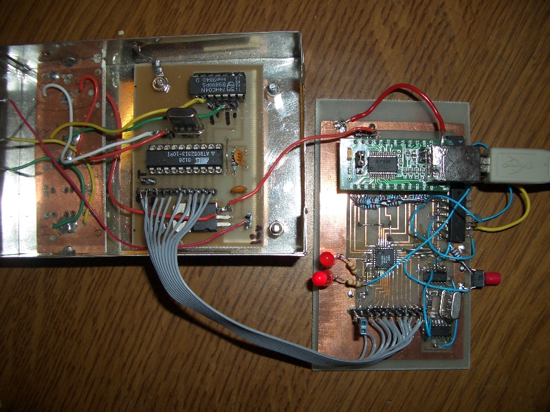
Current Setup (V2) with 70cm PLL VCO and modulator connected up - 14-1-2010
Current setup![]()
Improved constellation at 1Ms/s with new serialiser, see original on F4DAY info page..
IQ (XY) Scope plot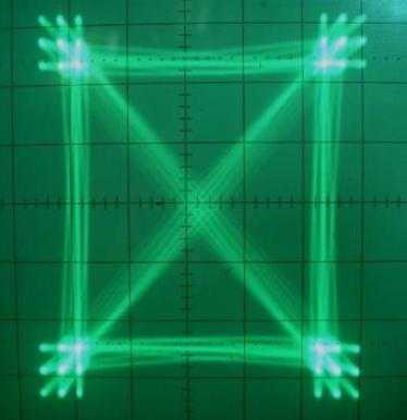
Related documents:
IDT7221 PDF
UM245 PDF


